“The Open Competition Mechanism To Select The Best Candidates” Stimulates The Vitality Of Scientific And Technological Innovation, SiC MOSFET Of Global Power Technology Co., Ltd Has Made A Breakthrou
The third-generation semiconductor silicon carbide power devices have the advantages of high voltage resistance, high temperature resistance and high energy conversion efficiency, and have broad application prospects in many fields such as new energy vehicles, photovoltaic power generation and rail transit. China's silicon carbide industry is still in the development stage of core technology research, and the localization process is imminent. In view of the "stuck neck" problem of silicon carbide power device research and development and the challenge of industrialization, the second batch of core technology research organized and implemented by the Science and Technology City Management Committee of Changsha Yuelu Mountain University "The Open Competition Mechanism To Select The Best Candidates" "high-power silicon carbide MOSFET and SBD chip technology research" project, which was issued by Liuyang Global Power Technology Co., Ltd(GPT), Hunan University and Dongguan Tianyu Semiconductor Co., Ltd. jointly unveiled, and multi-party cooperation to carry out technical research.

The project has been implemented for more than a year, and it is progressing smoothly with remarkable results. In view of the difficulty of this topic, the research part of silicon carbide MOSFET chip, the Hunan University team boldly abandoned the traditional planar gate structure in the design process, and proposed a new structure of field-plate separation SiC MOSFET, while GPT broke through the process difficulties such as high-quality gate oxygen treatment, surface passivization, and high-temperature variable energy multiple ion implantation, and completed the tape-out work based on its 6-inch silicon carbide wafer production line in Changsha. GPT's engineering team has demonstrated deep silicon carbide process capabilities, and the consistency and stability of batch tape-outs have been unanimously recognized by experts, laying a solid foundation for mass production.
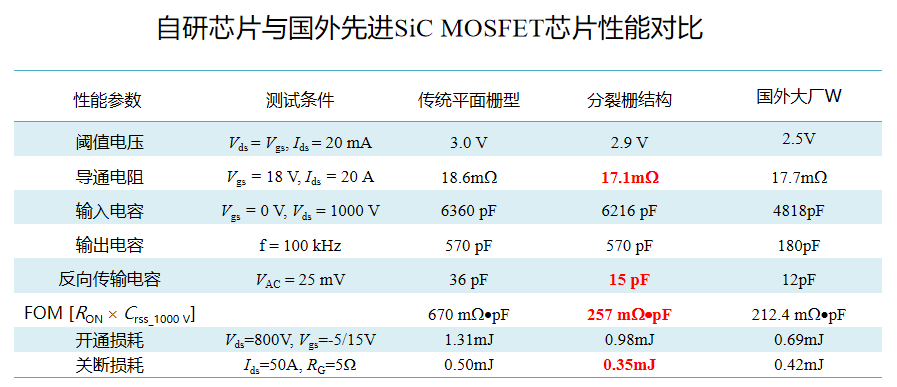
Due to the introduction of the split-gate structure of the field-plate separation type, the chip has a lower reverse transmission capacitance (Crss), and the high-frequency superior value HF-FOM [RON × CRSS] is close to the foreign advanced level, which is significantly improved compared with the traditional planar gate structure device index value. The electrical characteristics test results show that the on-resistance of the 5mm × 5mm SiC MOSFET chip is 17.1mΩ, which is consistent or slightly better than the on-resistance of similar products of foreign manufacturers of international SiC leading enterprises. At the same time, the total chip area after this tape-out is smaller than similar products on the market (26mm2), which can effectively reduce the cost of device manufacturing. Under the working condition of VDS=800V/IDS=50A, it is found that the switching performance of this batch of chips has been improved, and the turn-off loss is 0.35mJ, which is 17% lower than the shutdown loss (0.42mJ) of similar products of foreign manufacturers under the same working conditions, which will effectively improve the power conversion efficiency, which is reflected in downstream applications such as new energy vehicles, which will help improve the cruising range of electric vehicles.

The overall progress of the project was ahead of the expected timeliness, and the above phased results were achieved, laying a good foundation for the final success. Next, all parties will continue to deepen cooperation, continue to optimize and improve the performance of SiC devices, improve the stability of the preparation process, strive to achieve stable mass production of related products as soon as possible, and further enhance the influence of our province in the third-generation semiconductor industry.